- 您现在的位置:买卖IC网 > Sheet目录356 > SC618ULTRT (Semtech)IC LED DRIVER PHOTO FLASH 10-MLP
�� �
�
�NOT� RECOMMENDED� FOR� NEW� DESIGN�
�Applications� Information� (continued)�
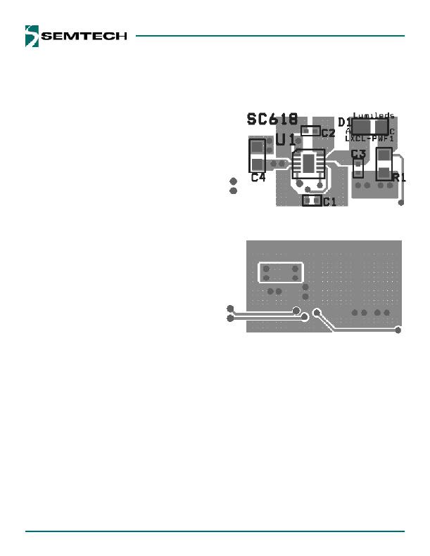
�SC618�
�PCB� Layout� Considerations�
�The� following� layout� is� suggested� for� a� two-layer� design.�
�The� capacitors� C1� and� C2� are� the� bucket� capacitors� and�
�while� in� flash� or� spotlight� mode.� It� is� critical� to� maintain�
�adequate� ground� plane� around� the� device� to� maximize�
�heat� transfer� and� avoid� over-temperature� shutdown.�
�each� conducts� the� full� load� current� of� up� to� 500mA� pulsed�
�for� one� half� clock� cycle.� C3� is� the� output� decoupling�
�capacitor� placed� near� the� VOUT� pin.� C4� is� the� input�
�decoupling� capacitor� placed� near� the� VIN� pin.� Multiple�
�vias� should� be� used� whenever� it� is� necessary� to� change�
�layers� on� nets� connecting� to� pins� VIN,� VOUT,� GND,� C1-,�
�C1+,� C2-� and� C2+.�
�The� load� current� return� path� is� from� the� ISET� sense� point�
�through� the� resistor� and� back� to� the� ground� pins.�
�Resistance� in� this� path� adds� to� the� total� resistance� and�
�has� the� effect� of� reducing� the� LED� current� by� about� 4%�
�per� 10mV� of� DC� drop� across� the� return� copper� trace� in�
�flash� mode.� For� this� reason,� it� is� crucial� to� have� a� low� resis-�
�tance� return� path.� Place� and� ground� the� resistor� as� close�
�as� possible� to� the� ground� pin� of� the� SC618.� The� trace� from�
�the� ISET� pin� has� virtually� no� current.� The� ISET� trace� should�
�make� contact� at� the� pad� of� the� power� sense� resistor� to�
�minimize� the� effect� of� voltage� drop� between� the� LED�
�cathode� and� the� resistor.�
�Resistor� R1� is� routed� with� a� very� low� resistance� connec-�
�tion� between� R1� and� GND� pin� 3.� The� sense� trace� between�
�Pin� 6� and� R1� is� routed� around� the� ground� vias,� allowing�
�the� shortest� ground� return� path� possible.� The� sense� trace�
�is� connected� to� R1� at� the� positive� terminal� pad� for� the�
�most� accurate� output� possible.� The� bottom� copper� layer�
�is� mostly� a� ground� plane� with� no� obstructions� between�
�the� ground� vias.� The� smaller� rectangle� to� the� left� con-�
�nects� the� input� power� to� VIN� pin� 1� and� input� capacitor�
�C4.� The� two� traces� at� the� lower� left� are� for� logic� inputs�
�FLASH� and� CTRL.� The� trace� to� the� right� is� the� ISET� pin�
�sense� trace.� The� sense� trace� is� routed� out� of� the� path� of�
�the� returning� ground� current.�
�Thermal� Resistance� Considerations�
�The� SC618� package� is� thermally� effi� cient� when� the� circuit�
�board� layout� connects� the� thermal� pad� through� multiple�
�vias� to� the� ground� plane.� The� thermal� resistance� is� rated�
�at� 40°C/W,� and� this� rating� is� dependent� on� the� connec-�
�tion� between� the� thermal� pad� and� the� ground� plane.� The�
�layout� should� keep� the� junction� temperature� below� the�
�OTP� limit� while� operating� the� SC618� within� the� specified�
�electrical� conditions� for� I� OUT� and� V� ISET� .� A� poor� layout� may�
�allow� the� junction� temperature� to� reach� the� OTP� limit�
�11�
�发布紧急采购,3分钟左右您将得到回复。
相关PDF资料
SC620ULTRT
IC LED DRIVER LINEAR 16-MLPQ
SC628AULTRT
IC LED DRIVER
SC667ULTRT
IC LED DRVR LMU 7CH MLPQUT20
SC668ULTRT
IC LED DRVR LMU 8CH MLPQUT20
SDIN2B2-8G
IC INAND FLASH 8GB 169FBGA
SDK-DM3730-10-256512R
KIT DEV ZOOM FOR AM/DM37X
SDK-DM3730-20-256512R
KIT DEV ZOOM FOR AM/DM37X
SE162216
ENCLOSURE ASSY 6U X 19" X 16"
相关代理商/技术参数
SC619
制造商:SEMTECH 制造商全称:Semtech Corporation 功能描述:Charge Pump Flash LED Driver with Safety Timer
SC619_08
制造商:SEMTECH 制造商全称:Semtech Corporation 功能描述:Charge Pump Flash LED Driver with Safety Timer
SC619EVB
制造商:SEMTECH 制造商全称:Semtech Corporation 功能描述:Charge Pump Flash LED Driver with Safety Timer
SC619ULTRT
制造商:SEMTECH 制造商全称:Semtech Corporation 功能描述:Charge Pump Flash LED Driver with Safety Timer
SC620
功能描述:UPS - 不间断电源 620VA/390W 4 Outlet
RoHS:否 制造商:Phoenix Contact 功率额定值: 输出电压额定值:24 V 出口数量:2 运行时间(满载): 运行时间(半载):
SC620 RPL
制造商:Schneider Electric 功能描述:REPAIR/REPLACE - Bulk
SC620_07
制造商:SEMTECH 制造商全称:Semtech Corporation 功能描述:Octal LED Driver, General Purpose Current Sink with Serial Interface
SC620_09
制造商:SEMTECH 制造商全称:Semtech Corporation 功能描述:Octal LED Driver,General Purpose Current Sink With Serial Interface